De-Featured DC load
Background
The story starts on a Saturday evening somewhere back in 2015. I suddenly found myself in a situation where I needed a DC load capable of dissipating a couple of watts - without having one available, of course. After a dive into the parts bin, I came up with something rather minimalistic (corresponding blog post):
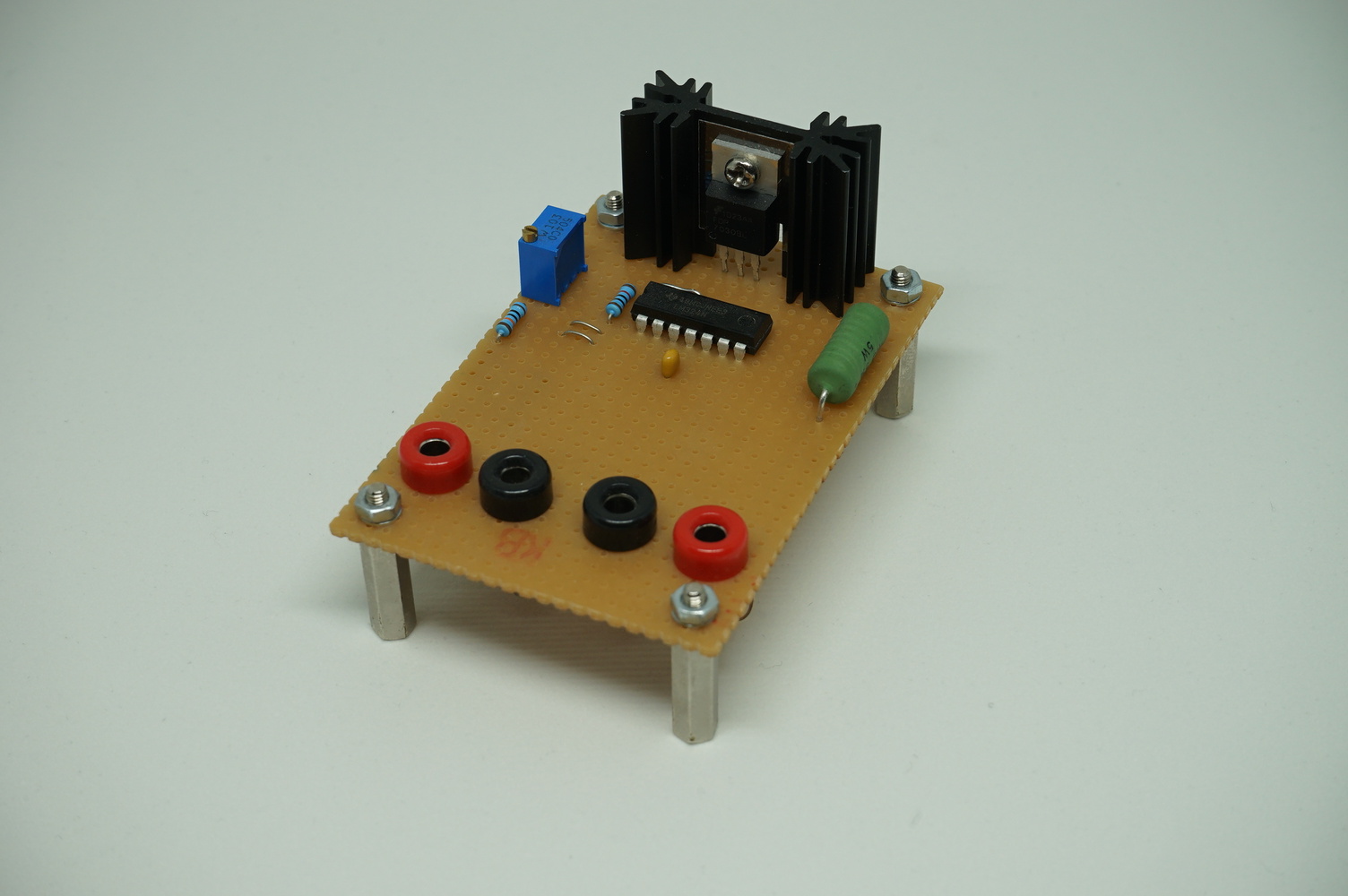
As this thing was sitting on my desk ever since I ended up using it way more frequently than I’d like to admit. The cheapest of commercially available DC loads does a better job than this thing but you know how it is… Furthermore, people that knew what they were looking at really like it as it was described as “cute” on several occasions. After seven years of (ab)use, I decided to give it the honors of making a proper PCB. I mainly took this opportunity to check out the latest version of KiCAD after many years of Altium usage.
Design
As with any good DIY project the design phase started off with an evening of feature creep. I considered adding some 7-segment display for set point & power reporting, automatic cut-offs and more. Eventually, I went back to the basics with the following requirements set out:
- No fancyness
- Completely analog
- At least 35W continuous power dissipation
- Easy to service
- Accommodate different MosFETs
- Retain the reported “cuteness” of the previous version
As such, the resulting device is as simple as it gets from any practical point of view. It is more or less a text book example suitable for any electronics novice to understand, build, troubleshoot and maintain.
One “feature” I added was an on-board fuse. An ATO/FKS fuse style was chosen as the popular 20x5mm format is either difficult or impossible to get in >10A ratings. While a typical household, office or lab might not have ATO/FKS style fuses in stock they are available in bulk from any electronics or car parts supplier.
The design is mostly centered around the LM324 - A quad OpAmp so notorious that one could easily source in >1k units during the worst of the supply chain pandemic. Two of these chips are used. Out of the eight available OpAmps six are used. This might be considered wasteful in a high-volume production scenario but keeping the unique parts count down is more relevant in a potentially one-off DIY project. Who doesn’t keep a tube of LM324s under their pillow at all times anyway?
As for the MosFET, I decided to keep the original choice of an N-Channel MosFET in a TO-220 package. This is not the most ideal choice and in retrospect I should have added a footprint that also fits a TO-263 (D2PACK) but getting any N-Channel MosFET in a TO-220 package is usually an easy task. Especially if you keep plenty of them around for your personal stock.
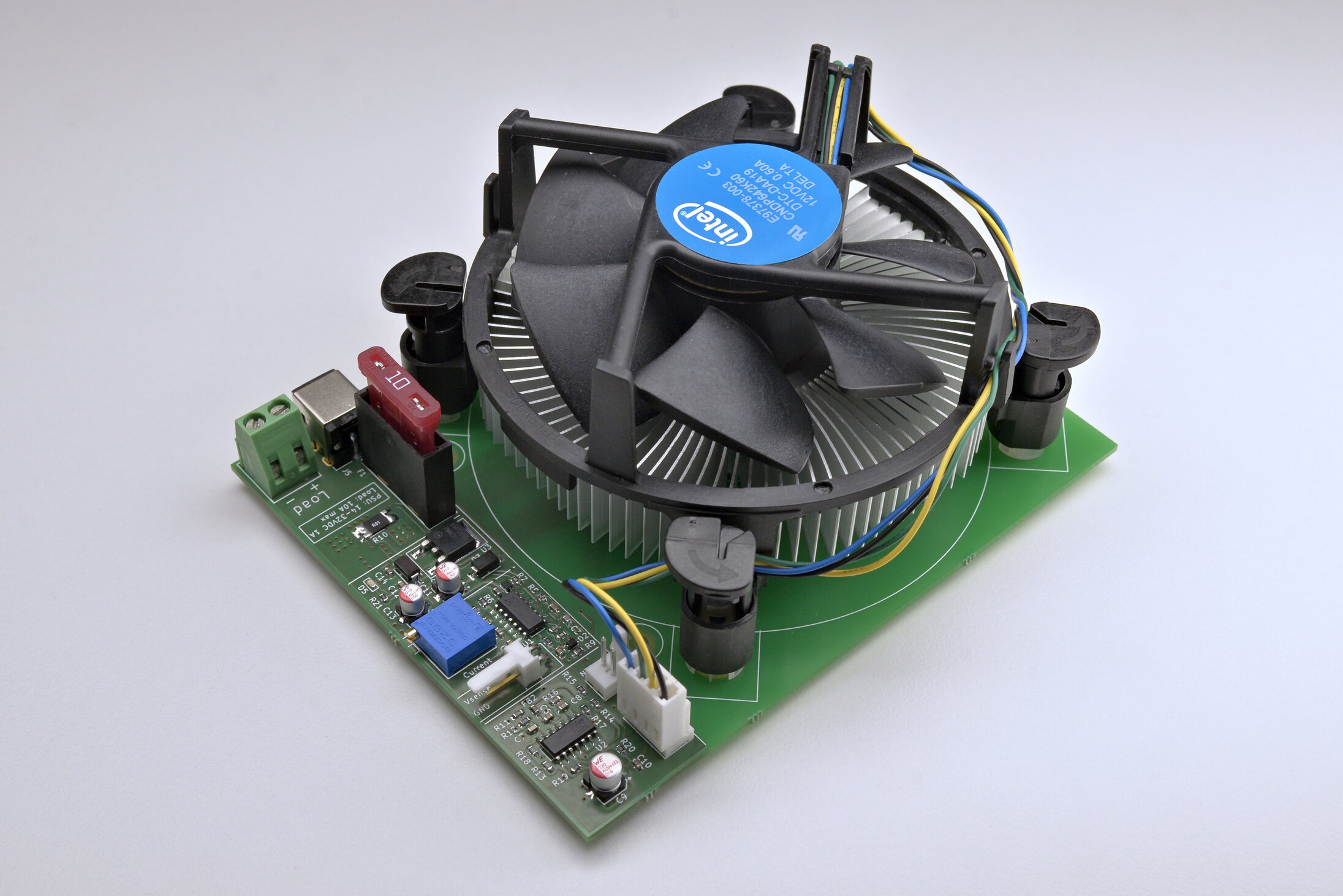
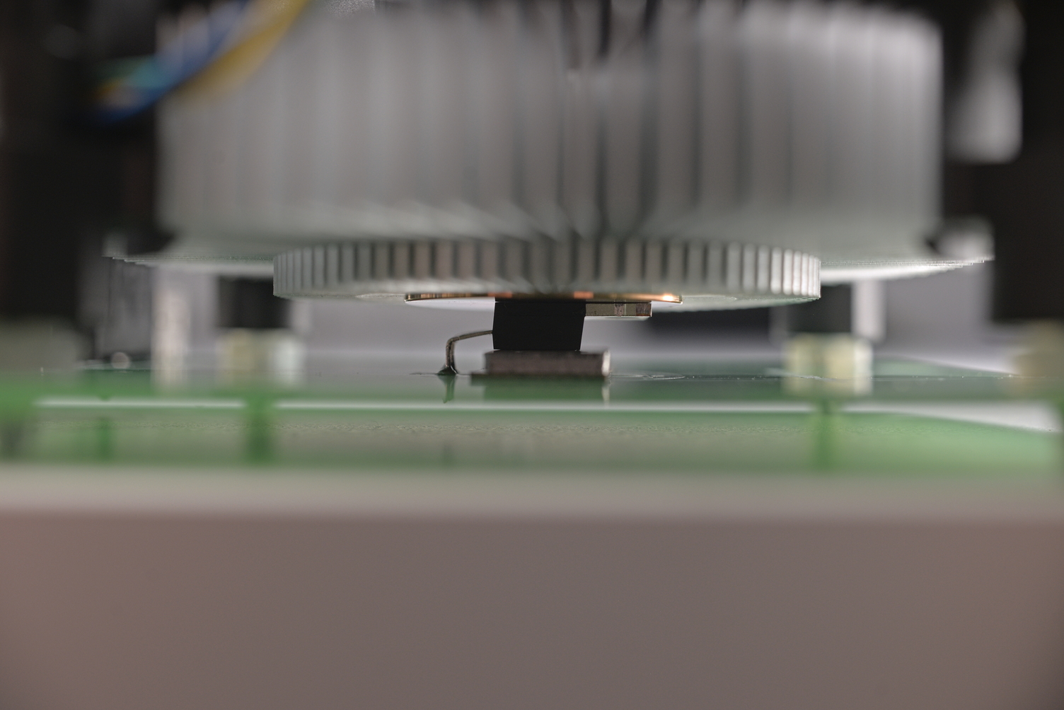
Several solutions were considered for the heatsink. Eventually, I settled on a stock Intel CPU cooler for the LGA-115x socket. I had some lying around but they are cheap to acquire otherwise. Furthermore, any Intel LGA-115x cooler is compatible with the design.
The result looks like this:
Schematics
The device consists of four main parts which are neatly separated on the PCB:
- Load path
- Power supply
- Control circuitry
- Fan control
Most components are not needed for the operation of this device while adding a few more components would have provided some improvements. This weird mix of choices is the result of keeping the parts requirements for the core functionality at a minimum. For example, the circuit would benefit from a lower voltage supply to increase sensitivity. However, the choice of supporting a 12V fan would have required adding an additional voltage regular which might not be optional. Adding some extra de-coupling capacitors, some clamping zener diodes, a power indicator LED and a simple sense circuit are optional parts which may be omitted with the device still being functional.
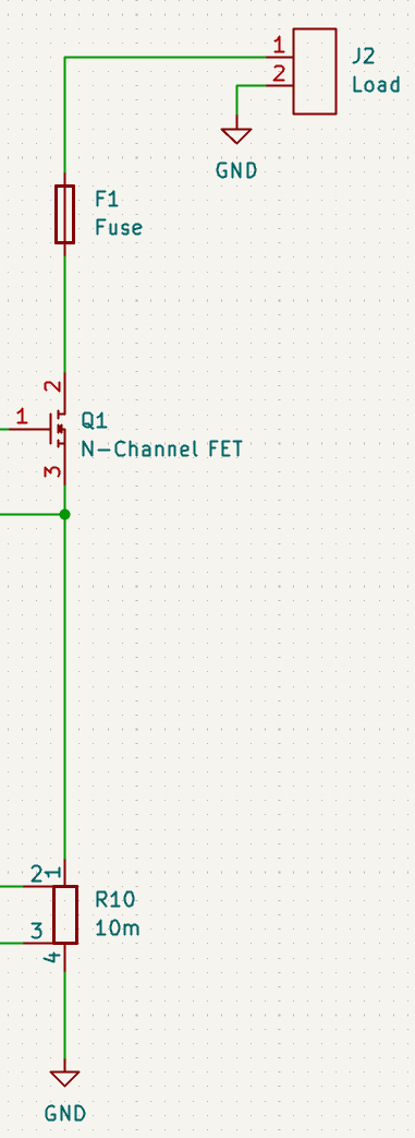
Load path
The load path is as simple as it gets. It consists of a screw terminal, an in-line fuse, the MosFET to convert electrical energy into thermal energy and a shunt resistor to optionally provide a sense port:
Power supply
The power supply consists of a simple linear 7812 regulator:
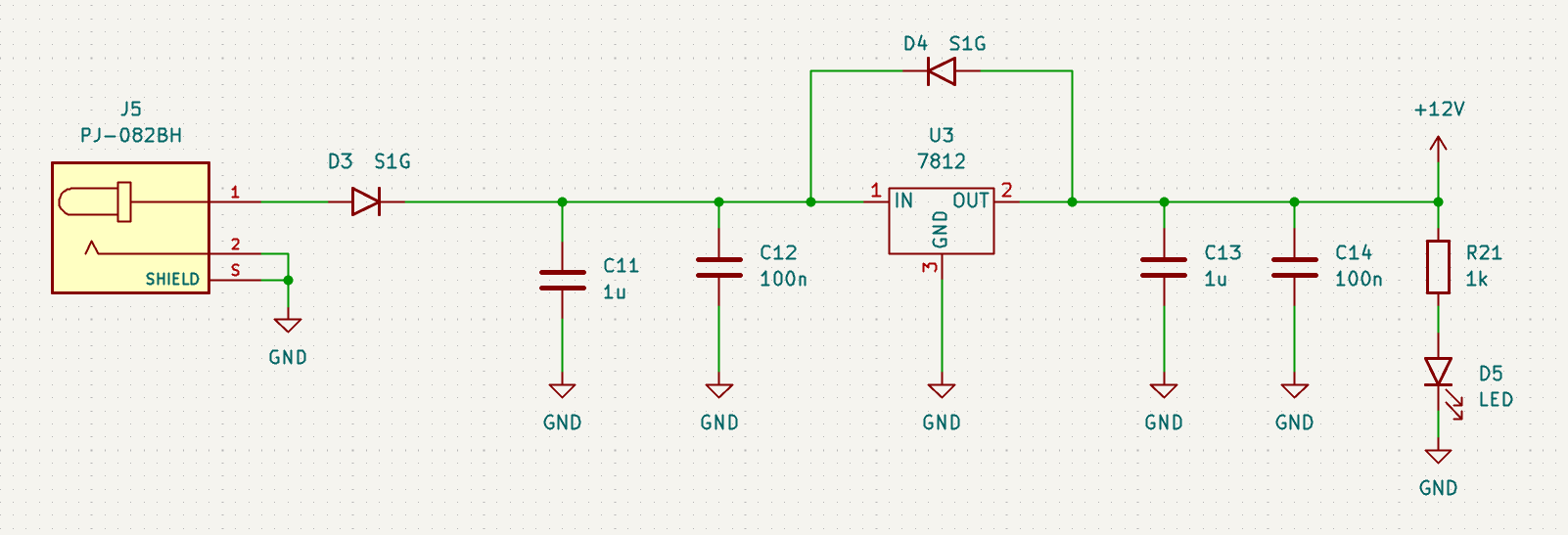
D4, C12 and C14 are pretty useless in this design but the board space was available.
Control circuitry
The control circuitry consists of two parts: An open-loop Gate-Source voltage controller and an amplifier to read back the voltage drop over the shunt:
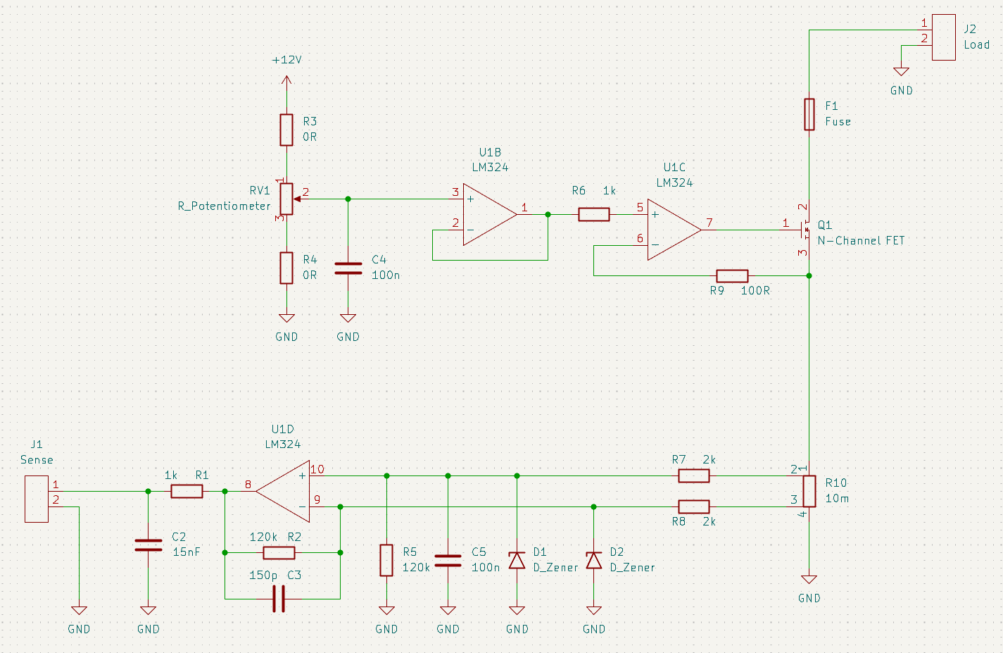
The voltage buffer in form of U1B is not exactly necessary but the OpAmp is in the package anyway so one might just as well use it.
R3 and R4 can be sized to limit the range of the trimmer RV1. This allows to utilize the full angular range of the trimmer in regards to varying Gate-Source voltages of different MosFETs and to counter the impact of the high voltage supply of 12V.
R2 and R5 determine the gain of the sense circuitry.
R1 and C2 implement a simple low-pass filter.
D1 and D2 are pretty useless in this particular design but again: Board space was available and DNP is always an option.
Spot the missing capacitor.
Fan control
Arguably the least de-featured feature of this entire device is an integrated temperature controlled fan speed controller for 4-Pin PWM fans.
With the spirit of keeping simple things simple, a PWM generator was built with a hand full of OpAmps in a way that the same LM324 could be used. A 10k NTC is used for the sensing element.
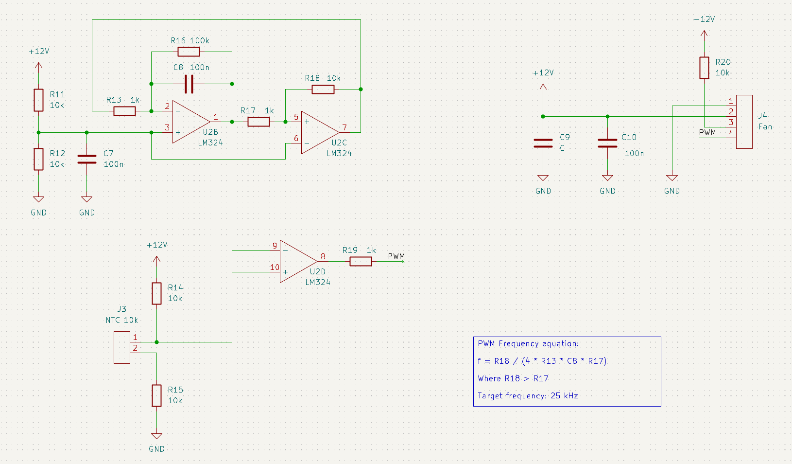
Similar to R3 and R4 of the control circuitry, R14 and R15 allow to limit the range of the NTC to facilitate different thermistors.
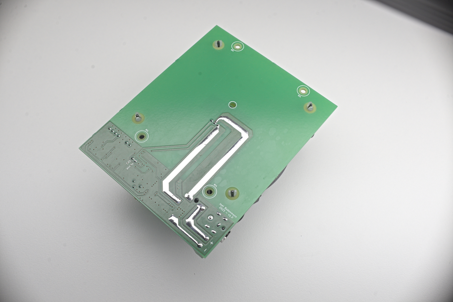
PCB
As with the circuit itself, the PCB was designed with easy manufacturing and repair in mind. Having done mostly 4 to 8 layer PCBs in recent years this two layer board presented a minor yet interesting reverse-challenge. The smallest track width is 0.3mm and the smallest hole size is 0.8mm which keeps the board well within your typical school/university and cheap PCB manufacturer capabilities.
The four sections of the circuit were separated neatly on the PCB:
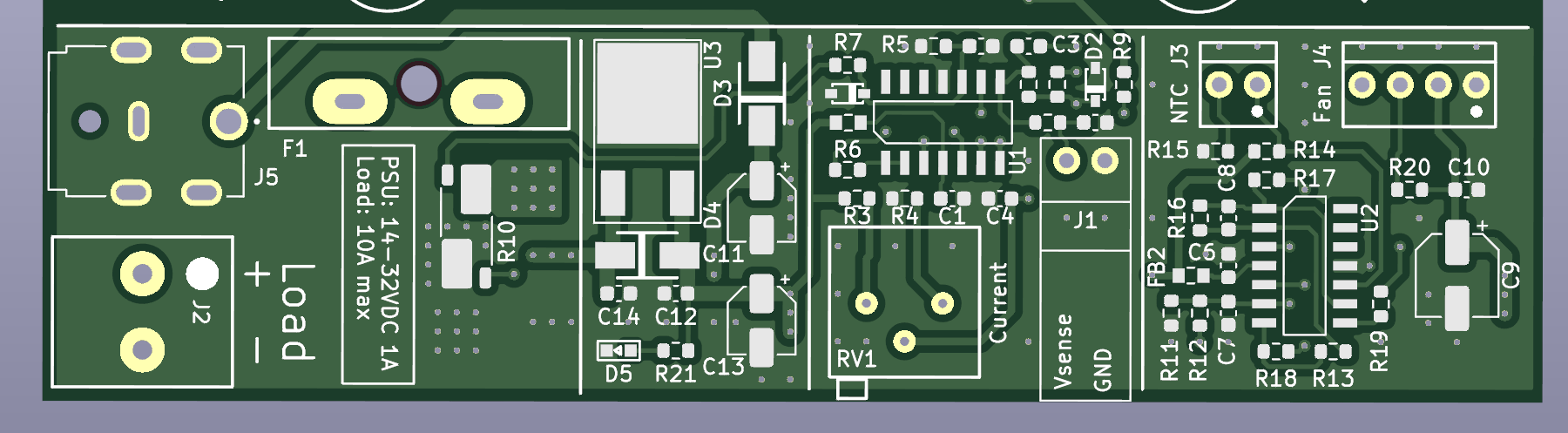
The solder mask of the power path traces was partially omitted to allow for increasing the current capabilities by slapping on some extra solder or optionally installing wires.
Mounting the TO-220 package upside down (with the metal tap facing up) allows for direct heat transfer to the heatsink. A shim between the PCB and the transistor fills the gap as the package isn’t thick enough to lie within the specification of the LGA-115x socket.
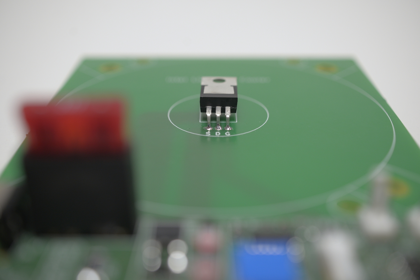
The gate-source voltage feedback is directly tapped off near the MosFET. Similarly, the taps for the shunt resistor voltage are directly routed to the resistor.
The only mishap that slipped through was labeling the four M3 mounting holes as M4 on the bottom silkscreen.
Conclusion
Could any cheap off-the-shelf DC load have done a similar or better job for less cost than this thing? Yes, definitely. But that is not what this was about.
The goal was to re-create the aestetics and servicability of the original design. Other than the readily available LM324 pretty much every component can be substituted for an alternative part or be omitted entirely while keeping the device functional. Furthermore, I didn’t do any non-professional PCB work the last few years so I enjoyed the freedom of fooling around a little. As such, I consider this project a success.
I plan to create a higher capacity DC load with more features (especially automatic cut-off) in the near future.
KiCAD files are available at GitHub.
Gallery